The heart of best pcb manufacturers in china fabrication lies in the precise transfer of the circuit design onto the copper layers. This is achieved through a combination of photoengraving and etching processes. The design is printed onto a light-sensitive film, which is then used to expose the copper layers to UV light. The unexposed areas are etched away, leaving behind the copper traces as per the circuit design.
Drilling and Plating:
Once the copper traces are etched, the board undergoes a drilling process to create holes for component placement and interconnections. To ensure electrical continuity, these holes are plated with a thin layer of copper, making them conductive. This step requires extreme precision, as the holes must align perfectly with the traces on various layers.
Solder Mask and Silkscreen:
To insulate and protect the copper traces, a solder mask is applied, leaving only the necessary contact points exposed. Additionally, a silkscreen layer is added to label components and provide essential information for assembly and troubleshooting.
Quality Control:
Throughout the entire PCB fabrication process, rigorous quality control checks are conducted. Automated optical inspection (AOI) and X-ray inspection are often used to identify any defects or deviations from the design. These inspections ensure the final product adheres to the highest quality standards.
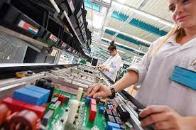
Testing and Assembly:
After successful fabrication, the PCBs undergo functional testing to verify their performance. They are then ready for component assembly. Surface mount technology (SMT) or through-hole technology (THT) are used to attach the components to the board, depending on the design and specifications.
The Final Product:
Once the components are secured, the PCB is ready for integration into the final electronic product. It serves as the central nervous system of devices, enabling the flow of data and power between various components and ensuring the proper functioning of the entire system.